Laser total cutting

Compound semiconductors such as GaAs (gallium arsenide) are used in high frequency devices. When using the existing diamond blade to cut compound semiconductor, the feed speed is slow and it is difficult to obtain high productivity.

With the trend of high integration, high-strength thin chip manufacturing technology based on SIP (system in package) and other technologies has become necessary. However, with the use of blade cutting, the cutting difficulty increases as the wafer thickness becomes thinner.

To solve these problems, disco optimized the laser head and optical system of dfl7161 laser saw, and established the application of laser full cutting.


Application

Laser full cutting technology

The process includes feeding the laser to the front (pattern side) of the thinned wafer (less than 200 µ m) once, or irradiating the wafer multiple times until the tape is cut. Laser full cutting can increase the output because it can increase the feed speed.

应用1.png

Process example

Thin wafer cutting of GaAs compound semiconductor

In the cutting process, GaAs wafer is easy to be damaged and cracked because the material is very brittle. Therefore, it is difficult to use the existing blade to improve the cutting speed. Using laser full cutting, processing can be carried out at a feed speed ten times faster than blade cutting, so as to improve the output. (this is just an example. The actual speed depends on the wafer to be processed.)

应用2.jpg

SEM image of GaAs wafer

* When processing GaAs, additional equipment is required to remove vaporized as gas.

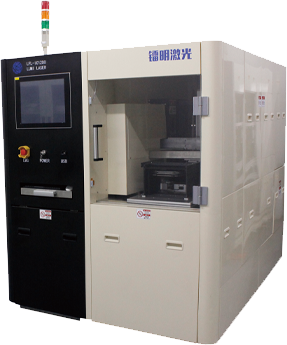
Thinning silicon wafer full cutting and scribing

As the wafer becomes thinner, the fragmentation and cracking in the cutting process have a greater impact on the chip strength. Therefore, the difficulty of cutting is increasing because of the need to better control the process of fragmentation. In addition, the number of devices using chip film (DAF) as bonding material to stack thinned chips is increasing. Therefore, while controlling the occurrence of burrs, high-quality cutting of wafers with DAF on the back has become a problem.

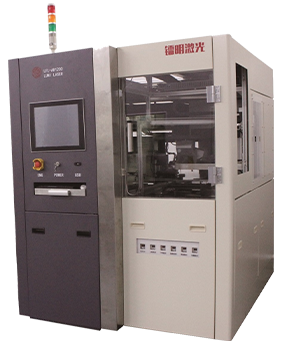
Other examples of laser full cutting

The back metal film is attached with silicon wafer, gap (gallium phosphide) wafer, InP (indium phosphide) wafer, Gan (gallium nitride) wafer and Ge (germanium) wafer.

应用3.jpg

关键词:硅晶圆

Cooperate with us to restore the appearance of your product blueprint!

Contact us
热推产品  |  主营区域: 江苏 上海 昆山 太仓 苏州
Home Telephone Message

Telephone

18651420821

Wechat

二维码

Pay attention to wechat

Consulting

TOP

Message

Please fill in your information correctly so that we can contact you at the first time