
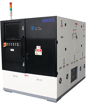
太仓Automatic laser debonding equipment
Model:Laser Grooving LFL-AB1200
Scope of application:Lowk wafer, Gan wafer, non low k wafer
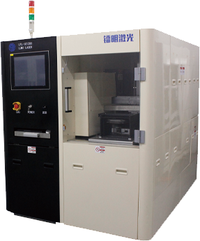
Model:Laser Grooving LFL-AB1200
Scope of application:Lowk wafer, Gan wafer, non low k wafer
With the continuous improvement of chip integration, the linewidth is getting smaller and smaller, and RC delay and crosstalk noise have become prominent problems. When the linewidth required by the process is less than 65nm, lon-k layer with low dielectric constant must be used to solve the above problems. Because it is difficult to use ordinary diamond grinding wheel for cutting, sometimes it can not meet the processing standards required by electronic component manufacturers. Therefore, the engineers of Suzhou radium laser technology Co., Ltd. have developed processing application technology that can solve this problem.
01. DPSS laser
02. Low damage and high yield
03. High precision and high speed debonding system
04. Spot detection and power feedback
05. Machinable size: 8inch and 12inch
06. Provide a complete set of solutions including bonding materials, processes and lasers
| Laser power | ≥15W(Measured about 18W) | ||
| Y-axis of linear motor | Stroke: 450mm | Stepping:1um | Resolution:1um |
| X-axis of linear motor | Stroke: 650mm | Stepping:1um | Resolution:1um |
| Z axis | Stroke: 20mm | Stepping:1um | Resolution:1um |
| θ axis | Stroke: 270° | Stepping:0.001° | Resolution:0.001° |
| Machining dimension | Maximum 12inch (300mm) | ||
| Scribing mode | Full cut / surface grooving | ||

Cooperate with us to restore the appearance of your product blueprint!
Contact usTel:18651420821
Email:lumi_server@lumilaser.com
Address:Building 4, Northwest District, nano City, No. 99, Jinjihu Avenue, Suzhou Industrial Park


Copyright © 2018 lumi laser. All rights reserved. Suzhou Laiming Laser Technology Co., Ltd ICP:苏ICP备2021045377-1
 Home
Home Telephone
 Message


